How Solar Energy Could Transform Online Gambling Into a Sustainable Industry
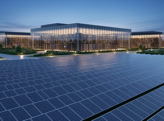
The online gambling industry faces mounting pressure to address its substantial carbon footprint, with platforms like Moonbet online casino and similar operators consuming massive amounts of electricity to power 24/7 data centers, streaming services, and transaction processing systems. As global data center energy consumption reaches 200 terawatt-hours annually—roughly 1% of worldwide electricity demand—gambling platforms that operate continuously represent a significant portion of this digital infrastructure load.
Solar photovoltaic systems offer gambling operators a strategic pathway to …